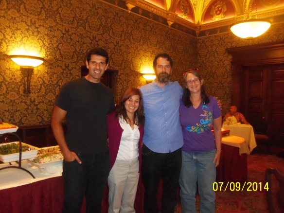
Sitting and eating lunch in the room where Einstein and many others of turbo charged, ultra-powered acumen sat and ate lunch excites me. So, I was thrilled when lunch was arranged for the teachers participating in IQIM’s Summer Research Internship at the famed Athenaeum on Caltech’s campus. Spyridon Michalakis (Spiros), Jackie O’Sullivan, Eryn Walsh and I were having lunch when I asked Spiros about one of the renowned “Millennium” problems in Mathematical Physics I heard he had solved. He told me about his 18 month epic journey (surely an extremely condensed version) to solve a problem pertaining to the Quantum Hall effect. Understandably, within this journey lied many trials and tribulations ranging from feelings of self loathing and pessimistic resignation to dealing with tragic disappointment that comes from the realization that a victory celebration was much ado about nothing because the solution wasn’t correct. An unveiling of your true humanity and the lengths one can push themselves to find a solution. Three points struck me from this conversation. First, there’s a necessity for a love of the pain that tends to accompany a dogged determinism for a solution. Secondly, the idea that a person’s humanity is exposed, at least to some degree, when accepting a challenge of this caliber and then refusing to accept failure with an almost supernatural steadfastness towards a solution. Lastly, the Quantum Hall effect. The first two on the list are ideas I often ponder as a teacher and student, and probably lends itself to more of a philosophical discussion, which I do find very interesting, however, will not be the focus of this posting.
The Yeh research group, which I gratefully have been allowed to join the last three summers, researches (among other things) different applications of graphene encompassing the growth of graphene, high efficiency graphene solar cells, graphene component fabrication and strain engineering of graphene where, coincidentally for the latter, the quantum Hall effect takes center stage. The quantum Hall effect now had my attention and I felt it necessary to learn something, anything, about this recently recurring topic. The quantum Hall effect is something I had put very little thought into and if you are like I was, you’ve heard about it, but surely couldn’t explain even the basics to someone. I now know something on the subject and, hopefully, after reading this post you too will know something about the very basics of both the classical and the quantum Hall effect, and maybe experience a spark of interest regarding graphene’s fascinating ability to display the quantum Hall effect in a magnetic field-free environment.
Let’s start at the beginning with the Hall effect. Edwin Herbert Hall discovered the appropriately named effect in 1879. The Hall element in the diagram is a flat piece of conducting metal with a longitudinal current running through. When a magnetic field is introduced normal to the Hall element the charge carriers moving through the Hall element experience a Lorentz force. If we think of the current as being convention al (direction flow of positively charged ions), then the electrons (negative charge carriers) are traveling in the opposite direction of the green arrow shown in the diagram. Referring to the diagram and using the right hand rule you can conclude a buildup of electrons at the long bottom edge of the Hall element running parallel to the longitudinal current, and an opposing positively charged edge at the long top edge of the Hall element. This separation of charge will produce a transverse potential difference and is labeled on the diagram as Hall voltage (VH). Once the electric force (acting towards the positively charged edge perpendicular to both current and magnetic field) from the charge build up balances with the Lorentz force (opposing the electric force), the result is a negative charge carrier with a straight line trajectory in the opposite direction of the green arrow. Essentially, Hall conductance is the longitudinal current divided by the Hall voltage.
Now, let’s take a look at the quantum Hall effect. On February 5th, 1980 Klaus von Klitzing was investigating the Hall effect, in particular, the Hall conductance of a two-dimensional electron gas plane (2DEG) at very low temperatures around 4 Kelvin (- 4520 Fahrenheit). von Klitzing found when a magnetic field is applied normal to the 2DEG, and Hall conductance is graphed as a function of magnetic field strength, a staircase looking graph emerges. The discovery that earned von Klitzing’s Nobel Prize in 1985 was as unexpected as it is intriguing. For each step in the staircase the value of the function was an integer multiple of e2/h, where e is the elementary charge and h is Planck’s constant. Since conductance is the reciprocal of resistance we can view this data as h/ie2. When i (integer that describes each plateau) equals one, h/ie2 is approximately 26,000 ohms and serves as a superior standard of electrical resistance used worldwide to maintain and compare the unit of resistance.
Before discussing where graphene and the quantum Hall effect cross paths, let’s examine some extraordinary characteristics of graphene. Graphene is truly an amazing material for many reasons. We’ll look at size and scale things up a bit for fun. Graphene is one carbon atom thick, that’s 0.345 nanometers (0.000000000345 meters). Envision a one square centimeter sized graphene sheet, which is now regularly grown. Imagine, somehow, we could thicken the monolayer graphene sheet equal to that of a piece of printer paper (≈ 0.1 mm) while appropriately scaling up the area coverage. The graphene sheet that originally covered only one square centimeter would now cover an area of about 2900 meters by 2900 meters or roughly 1.8 miles by 1.8 miles. A paper thin sheet covering about 4 square miles. The Royal Swedish Academy of Sciences at nobelprize.org has an interesting way of scaling the tiny up to every day experience. They want you to picture a one square meter hammock made of graphene suspending a 4 kg cat, which represents the maximum weight such a sheet of graphene could support. The hammock would be nearly invisible, would weigh as much as one of the cat’s whiskers, and incredibly, would possess the strength to keep the cat suspended. If it were possible to make the exact hammock out of steel, its maximum load would be less than 1/100 the weight of the cat. Graphene is more than 100 times stronger than the strongest steel!
Graphene sheets possess many fascinating characteristics certainly not limited to mere size and strength. Experiments are being conducted at Caltech to study the electrical properties of graphene when draped over a field of gold nanoparticles; a discipline appropriately termed “strain engineering.” The peaks and valleys that form create strain in the graphene sheet, changing its electrical properties. The greater the curvature of the graphene over the peaks, the greater the strain. The electrons in graphene in regions experiencing strain behave as if they are in a magnetic field despite the fact that they are not. The electrons in regions experiencing the greatest strain behave as they would in extremely strong magnetic fields exceeding 300 tesla. For some perspective, the largest magnetic field ever created has been near 100 tesla and it only lasted for a few milliseconds. Additionally, graphene sheets under strain experience conductance plateaus very similar to those observed in the quantum Hall effect. This allows for great control of electrical properties by simply deforming the graphene sheet, effectively changing the amount of strain. The pseudo-magnetic field generated at room temperature by mere deformation of graphene is an extremely promising and exotic property that is bound to make graphene a key component in a plethora of future technologies.
Graphene and its incredibly fascinating properties make it very difficult to think of an area of technology where it won’t have a huge impact once incorporated. Caltech is at the forefront in research and development for graphene component fabrication, as well as the many aspects involved in the growth of high quality graphene. This summer I was involved in the latter and contributed a bit in setting up an experimen t that will attempt to grow graphene in a unique way. My contribution included the set-up of the stepper motor (pictured to the right) and its controls, so that it would very slowly travel down the tube in an attempt to grow a long strip of graphene. If Caltech scientist David Boyd and graduate student Chen-Chih Hsu are able to grow the long strips of graphene, this will mark yet another landmark achievement for them and Caltech in graphene research, bringing all of us closer to technologies such as flexible electronics, synthetic nerve cells, 500-mile range Tesla cars and batteries that allow us to stream Netflix on smartphones for weeks on end.


